WHY THIS MATTERS IN BRIEF
Metalenses are revolutionary – they’re nano-thin and flat which makes them the future of camera technology, now they could be manufactured at millionths of cents on the dollar.
 Interested in the Exponential Future? Join our XPotential Community, future proof yourself with courses from our XPotential Academy, connect, watch a keynote, or browse my blog.
All the cameras you use today use glass lenses, and by future standards are ginormous and bulky – all cameras that is except this revolutionary AI camera that doesn’t have any lenses at all. Today though we have camera’s that are so tiny they can travel through your blood vessels, and elsewhere new metalenses, which could one day help us create nano-thin cameras and hi def Virtual Reality glasses, as well as invisibility cloaks – even though we already have those thanks to another to another technology, namely metamaterials – have also been gaining ground.
Metalenses are special because they’re incredibly tiny, nanoscale tiny, and they’re flat which ultimately means you could create a smartphone camera that’s just atoms thick. However, as promising as they are up until now figuring out a way to manufacture them at scale and cheaply enough has been a challenge. Now though that’s all about to change after researchers figured out a way to make them using the same process we make computer chips, according to a new study (Nano Lett. 2019, DOI: 10.1021/acs.nanolett.9b03333).
Today’s cell phone lenses are made of plastic and curved, and many are stacked together to get the right optical performance. Such setups are thicker and require alignment. Making lenses wider would allow them to take in more light, but then they would also produce more aberrations, which would require weighty, more complex setups to compensate.
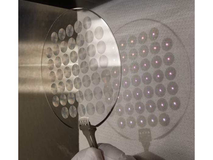
A fused silica wafer contains 45 metalenses, each 1 cm in diameter. Credit: Nano Lett.
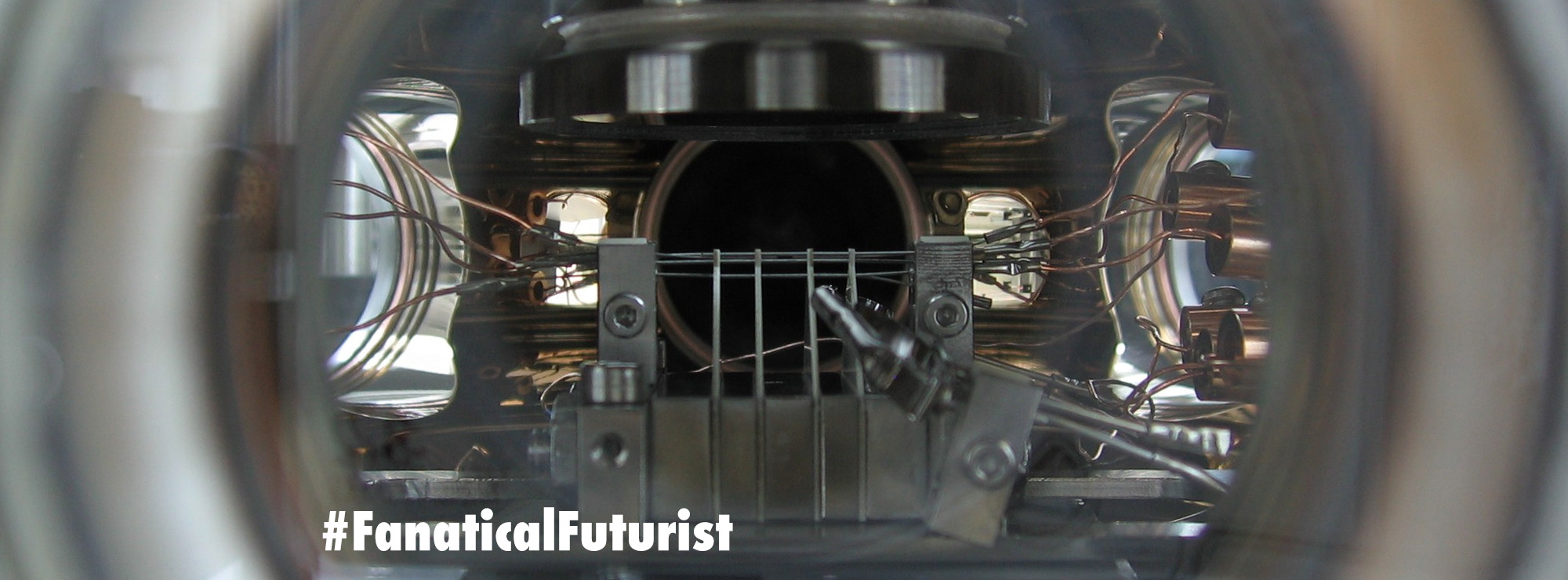
Metalenses bypass the need for curves – instead of relying on the inherent refracting power of the lens material they are based on metasurfaces, thin pieces of material studded with nano structures that manipulate light based on their size and arrangement. Researchers have used electron-beam lithography to create such nanostructures on thin films, but that process is slow and not suitable for mass production. Now, Federico Capasso, a physicist at Harvard University, and his colleagues have built a metalens using Deep-Ultraviolet (DUV) projection lithography, the same technology that mass-produces computer chips, as well as the light detectors used in most cell phone cameras.
The group built 45 metalenses, each 1 cm in diameter, on a wafer made of fused silica, a type of glass. Using standard DUV lithography processes, the researchers etched 160 million nanopillars – 2 µm tall and of various diameters – arrayed in a radial pattern so that light hitting the lens focuses down to the theoretical limit. Materials with a high dielectric index such as silicon, titanium dioxide, silicon nitride, or gallium nitride would also work but would involve extra processing steps. “We decided to use the simplest possible material,” Capasso says.
The biggest obstacle came in creating a design file that the lithography equipment could handle, says Joon-Suh Park, a graduate student in Capasso’s lab. The researchers had to create a compression algorithm that could shrink the complex designs with the varying dimensions and specific locations of the pillars to a manageable size.
The researchers designed the pattern on the metasurface lenses to focus 633 nm light, but the lenses could focus various visible wavelengths down to their theoretical limit at different focal lengths.
Because glass is made of silicon, the same material used to make everything else in a silicon wafer fabrication facility, there’s no worry about introducing a material that could contaminate other processes, Capasso says. Flat metalenses require less material than curved lenses and so will be lower weight, which could be important for optics in applications such as unmanned aerial vehicles and satellites. Also, they don’t suffer from increasing aberrations as their diameters increase, the way refractive lenses do. And aligning metalenses on top of camera sensors should be easier than for typical curved lenses.
Yujie Chen, an optical engineer at Sun Yat-sen University, calls this a “nice piece of work” that shows DUV lithography is feasible for mass-producing metalenses. Chen points out that glass metalenses can only capture light over a narrow range of angles because of the material’s relatively low refractive index. Using silicon nitride or titanium dioxide, which both have higher refractive indexes, would overcome that limitation. “Such materials can be compatible with the DUV projection lithography fabrication process,” Chen says.