WHY THIS MATTERS IN BRIEF
Particle accelerators are useful for all kinds of things, from finding new particles to helping build better semiconductors, and now we have a way to miniaturise them and put them on a chip.
 Interested in the Exponential Future? Connect, download a free E-Book, watch a keynote, or browse my blog.
A while ago I discussed how a group of scientists from Stanford University in the US were involved in an ambitious “Particle accelerator on a chip” project that, back in the day, would let them pack the power of a 3.2km particle accelerator into as little as 30 meters. Now almost two years into their five year project the team behind the project have an update and have announced they’ve made significant progress in their attempt to cram a SLAC sized particle accelerator onto something no larger than a computer chip.
In a full-scale particle accelerator, electrons fly along a kilometers-long path as microwaves bombard them, boosting the particles to near light speed. Such a high-energy electron beam, produced at facilities such as California’s SLAC National Accelerator Laboratory, enables a variety of experiments, including capturing extremely detailed images and probing the structures of molecules. But particle accelerators are expensive, require scientists to travel from locations all over the world and cannot accommodate all the researchers who submit requests to book time. To make these devices more accessible, the Stanford team developed a laser driven particle accelerator that fit on a tiny silicon chip that could eventually be scaled up to produce a beam with as much energy as SLAC’s.
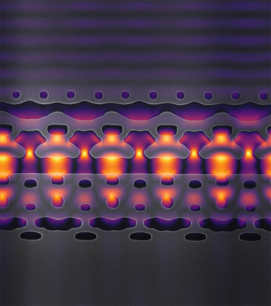
This image, magnified 25,000 times, shows a section of an accelerator-on-a-chip. The gray structures focus infrared laser light (shown in yellow and purple) on electrons flowing through the center channel. By packing 1,000 channels onto an inch-sized chip, Stanford researchers hope to accelerate electrons to 94 percent of the speed of light. (Image credit: Courtesy Neil Sapra)
“The idea of using lasers in accelerators goes all the way back to the year the laser was invented, 1960,” says Robert Byer, a Stanford researcher who has been working on this concept since 1974. Lasers produce electromagnetic waves with much shorter wavelengths than the microwaves used in a full-scale accelerator, which means they can accelerate electrons moving through a much smaller space. “The size of these devices is uncannily small,” Byer says. The electrons in the new accelerator, for example, travel along a channel that is about three one-thousandths of a millimeter wide -around half the width of a human red blood cell.
Although laser-driven devices can accelerate electrons in a much smaller space than full-scale accelerators, they also require much greater precision to line up the laser and the electrons in the right way, so the light waves push the particles in the correct direction with as much energy as possible.
“You not only have to demonstrate the ability to couple the laser light to the electrons in these very small structures, but you have to generate the electrons and have them also be transmitted by the channel,” Byer explains.
In 2013 two research groups, one at Stanford and other US institutions and another in Germany, independently managed to accelerate electrons with lasers. But these proof-of-concept prototypes required separate devices to generate the electrons, and they would be difficult to manufacture in bulk using existing techniques.
A laser driven accelerator engraved in silicon, however, would be easier to scale up, and multiple components could potentially fit on the same chip. Byer worked with several other researchers, including Stanford University electrical engineer Jelena Vuckovic, to produce such a tool.
“What you have to design is the structure that will guide light in the right way, so light will always provide a kick in the right direction—so particles are always getting accelerated,” Vuckovic says. To determine that structure, her student Neil Sapra used a computer to simulate how different patterns would interact with incoming electromagnetic waves. Once they had a design that accelerated the electrons as much as possible, and always did so in the right direction, the researchers etched this accelerator into a silicon wafer.
When the wafer is blasted with laser pulses from above, the laser light hits a grating called an “input coupler,” which sends it moving along the length of the chip. Next, the light waves run into the computer-designed path that cuts across the width of the chip. As the light passes through, the pattern focuses the waves, so they impart energy to a beam of electrons shooting along the path. This energy pushes the particles forward faster, and a description of the chip was published Thursday in Science.
“It’s a quite promising paper,” says Mark Palmer, director of the Accelerator Test Facility at Brookhaven National Laboratory, who was not involved in the new research. “I think they did a very nice job of showing how we can start to move forward with designing these structures and actually coming up with working devices, hopefully, in the not too distant future,” he adds.
The Stanford researchers found their prototype could successfully boost the electrons’ energy by 915 electron volts. Although that amount of energy is miniscule by everyday standards, the increase occurred as the electrons travelled only three one-hundredths of a millimetre – equivalent to them gaining about 30 million electron volts over the course of a meter. That change is not on the scale of what an accelerator like SLAC, which has many meters in which to power up its electrons by tens of billions of electron volts, can impart. The miniature accelerator can, however, scale up much more easily than its larger counterpart because it is etched in a small silicon wafer, researchers can fit multiple accelerating paths into future designs without adding bulk.
“We showed a single stage of the accelerator,” Vuckovic says. “It’s very simple scaling going from this single stage to 1,000 stages on a single silicon wafer.” She estimates that 1,000 stages could fit on a chip a couple of centimeters in length and imbue electrons with a million electron volts’ worth of energy, allowing them to travel at about 94 percent of the speed of light. That achievement would be enough for researchers to carry out some experiments that currently require visits to accelerators like SLAC.
Electrons with that amount of energy could also potentially enable medical applications, such as providing targeted radiation treatment for cancer patients without damaging healthy tissue.
“We can basically make instruments where we can have very tightly focused electron beams, and can use this to selectively target tumors,” Vuckovic says. She expects that her team could develop this scaled-up chip within a year, but that it may be about five years before the device can be used in practical applications, and even longer before it finds its way into medical treatments.
Palmer is more conservative with his estimates, guessing that applications may take 10 years to come to fruition. He is optimistic, however, about the impact accelerators on chips will have at that time. “At the end of the day, by [accelerating particles] in these small structures, you have devices that are readily adaptable to whatever environment you need to operate them in,” he says, “as opposed to having a much larger particle accelerator that has to go into a very fixed sort of footprint.”
Source: Stanford University