WHY THIS MATTERS IN BRIEF
Computer chips are prized assets, but now reverse engineering them and spotting state sponsored built in security “Trojans,” are easier than ever before.
Peering inside semiconductor chips using X-Ray imaging isn’t new, but the technique hasn’t been especially good or easy to accomplish. New advances reported by Swiss researchers in Nature recently now suggest that the practical use of X-Rays for fast, accurate, reverse engineering of chips may be near. And if your chips are your company’s IP, like they are Intel’s, or if advanced chip designs help prop up your country’s economy, like they do in the US, then that’s an issue. A big issue.
“You’ll pop in your chip and out comes the schematic. Total transparency in chip manufacturing is on the horizon,” said Anthony Levi of the University of Southern California describing the research in an IEEE Spectrum article, “this is going to force a rethink of what computing is, and what it means for a company to add value in the computing industry.”
The work by Mirko Holler, Manuel Guizar-Sicairos, Esther Tsai, Roberto Dinapoli, Elisabeth Müller, Oliver Bunk, Jörg Raabe, who are all from the Paul Scherrer Institut, and Gabriel Aeppli from ETH Zurich, is described in their Nature Letter, “High-resolution non-destructive three-dimensional imaging of integrated circuits.”
“[We] demonstrate that X-ray ptychography – a high-resolution coherent diffractive imaging technique – can create three-dimensional images of integrated circuits of known and unknown designs with a lateral resolution in all directions down to 14.6 nanometres. We obtained detailed device geometries and corresponding elemental maps, and show how the devices are integrated with each other to form the chip,” write the researchers in the abstract.
“Our experiments represent a major advance in chip inspection and reverse engineering over the traditional destructive electron microscopy and ion milling techniques. Foreseeable developments in X-ray sources optics and detectors, as well as adoption of an instrument geometry optimized for planar rather than cylindrical samples, could lead to a thousand-fold increase in efficiency, with concomitant reductions in scan times and voxel sizes.”
Starting with a known structure, an ASIC developed at the institute, and then moving to an Intel chip, the Intel G3260 processor, about which they had limited information, the researchers were able to accurately identify and map components in the chips.
A good summary of the experiment is provided in the IEEE Spectrum article:
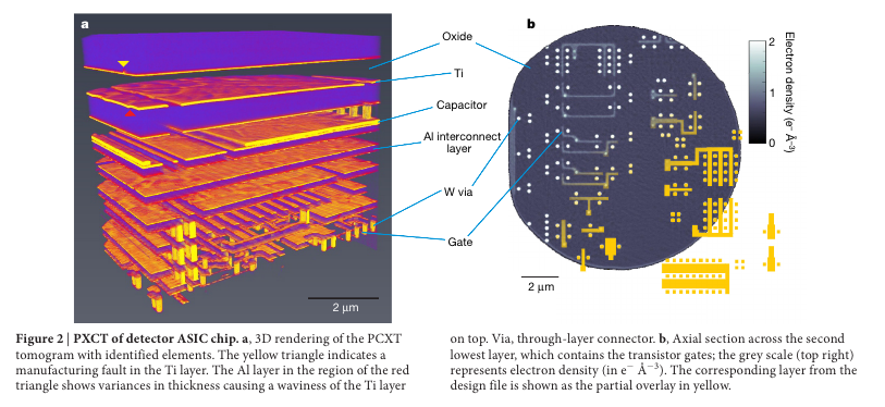
“The ASIC was produced using 110-nanometer chip manufacturing technology, more than a decade from being cutting edge. But the Intel chip was just a couple of generations behind the state of the art: It was produced using the company’s 22-nm process… To produce a 3D rendering of the Intel chip, an Intel G3260 processor, the team shined an X-Ray beam through a portion of the chip. The various circuit components – its copper wires and silicon transistors, for example – scatter the light in different ways and cause constructive and destructive interference. Through a technique called X-ray ptychography, the researchers could point the beam at their sample from a number of different angles and use the resulting diffraction patterns to reconstruct chip’s internal structure.”
The experiment was carried out at the cSAXS beamline of the Swiss Light Source (SLS) at the Paul Scherrer Institut, Villigen, Switzerland. Details of the components are as follows. Coherent X-Rays enter the instrument and pass optical elements that in their combination form an X-Ray lens used to generate a defined illumination of the sample. These elements are a gold central stop, a Fresnel zone plate and an order sorting aperture. The diffracted X-rays are measured by a 2D detector, a Pilatus 2M in the present case. Accurate sample positioning is essential in a scanning microscopy technique and is achieved by horizontal and vertical interferometers.
As the IEEE Spectrum article notes, “Even if this approach isn’t widely adopted to tear down competitors’ chips, it could find a use in other applications. One of those is verifying that a chip only has the features it is intended to have, and that a “hardware Trojan,” added circuitry that could be used for malicious purposes, hasn’t been introduced.”


Do it for FPGAs and then we can reverse the bitstream.
the bitstream usually sit on an external memory, easy to tap, but it’s encrypted. There must be substantial differences between an FPGA (that is RAM based AFAIK) and a ‘hard’ chip
Bitstream is well encrypted. it is as good as intellectual IP.
Nice, down to 14.6 nano scale, peek-a-boo @ possible embedded trojan.
Nice, down to 14.6 nano scale, peek-a-boo @ possible embedded trojan.
When can I get a PDP-8/L?
Thanks I just googled is it possible to reverse engineer a chip with imaging, and BAM. 😀 Encouraging. It should solve the crisis with Huawei if they can just spot inspect the chips, problem solved I think! 🙂