WHY THIS MATTERS IN BRIEF
We’re traditionally used to displays being bulky and stiff, but increasingly scientists are finding new ways to create new types of displays that break the status quo, and which will open up millions of new use cases, from health monitoring to way beyond.
We’ll soon be seeing the emergence of 11k displays from companies like Samsung that have what’s called a “naked eye” 3D effect, giant rollable displays from LG, and Panasonic, not to be left out, have also been doing their best to build displays that merge into the background, but now researchers from University of California Berkeley in the US engineers have built a bright light emitting device that is just mere millimeters wide and fully transparent when turned off, and people are already calling it one of the world’s first fully transparent displays. Furthermore the light emitting material in the device, which is something called a monolayer semiconductor, is just three atoms thick… and who knows, maybe if it’s combined with Harvard’s latest “Metalense” breakthrough it could even bring invisibility cloaks one step closer…
Not only does the new device open the door to create invisible displays that could be used on everything from walls and windows, that would be bright when turned on and see through when turned off, but it also paves the way for other more futuristic applications such as smart tattoos that, among other things, when combined with biomarkers, could give people visual indications about their health or a particular illness they’re suffering from.
“The material so thin and flexible that the device can be made transparent and flexible enough to flow around curved surfaces,” said Der-Hsien Lien, a postdoctoral fellow at UC Berkeley and a co-first author of the research which was published in the journal Nature Communications. The work was funded by the National Science Foundation and the US Department of Energy.
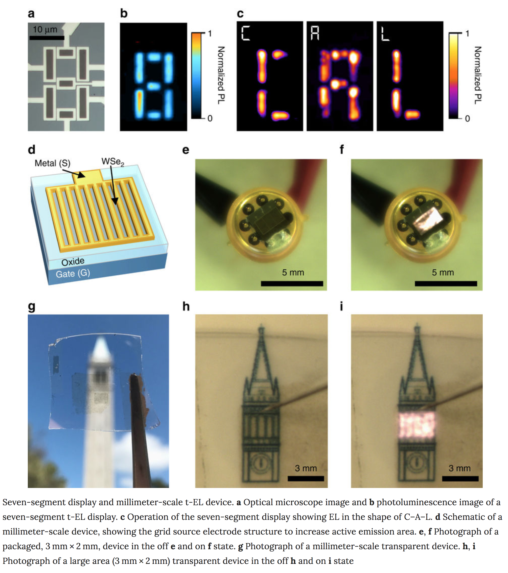
The device was developed in the laboratory of Ali Javey, professor of Electrical Engineering and Computer Sciences at Berkeley, and in 2015 he published research in the journal Science showing that monolayer semiconductors were capable of emitting bright light, but stopped short of building one. His latest work though overcame some of the fundamental barriers outlined in the original paper regarding using LED technology on monolayer semiconductors and let him scale them up from sizes smaller than the width of a human hair to several millimetres across while still retaining their thickness without, importantly, loosing any of the light’s intensity.
Commercial LEDs consist of a semiconductor material that is electrically injected with positive and negative charges, which produce light when they meet. Typically, two contact points are used in a semiconductor based light emitting device, one for injecting negatively charged particles and one injecting positively charged particles. Making contacts that can efficiently inject these charges is a fundamental challenge for LEDs, and it is particularly challenging for monolayer semiconductors since there is so little material to work with.
The Berkeley research team engineered a way to circumvent this challenge by designing a new device that only requires one contact on the semiconductor. By laying the semiconductor monolayer on an insulator and placing electrodes on the monolayer and underneath the insulator, the researchers could apply an AC signal across the insulator. During the moment when the AC signal switches its polarity from positive to negative, and vice versa, both positive and negative charges are present at the same time in the semiconductor, creating light.
The researchers also showed that this mechanism works in four different monolayer materials, all of which emit different colours of light.
For now though the new device is a proof of concept and there’s still a lot of research and testing to be done, primarily to improve the LED’s efficiency, which at the moment seems to sit at around the 1 percent mark compared to commercial LED’s whose efficiency is typically between 25 and 30 percent, before it can stand a shot of being commercialised and hitting the market.
“A lot of work remains to be done and a number of challenges need to be overcome to further advance the technology for practical applications,” said Javey, “however, this is one step forward by presenting a device architecture for easy injection of both charges into monolayer semiconductors.”