WHY THIS MATTERS IN BRIEF
As physical chip design starts to near its limits it is getting harder for companies to keep up with Moore’s Law but IBM’s latest announcement gives it a new shot in the arm – until that is Quantum Computing arrives.
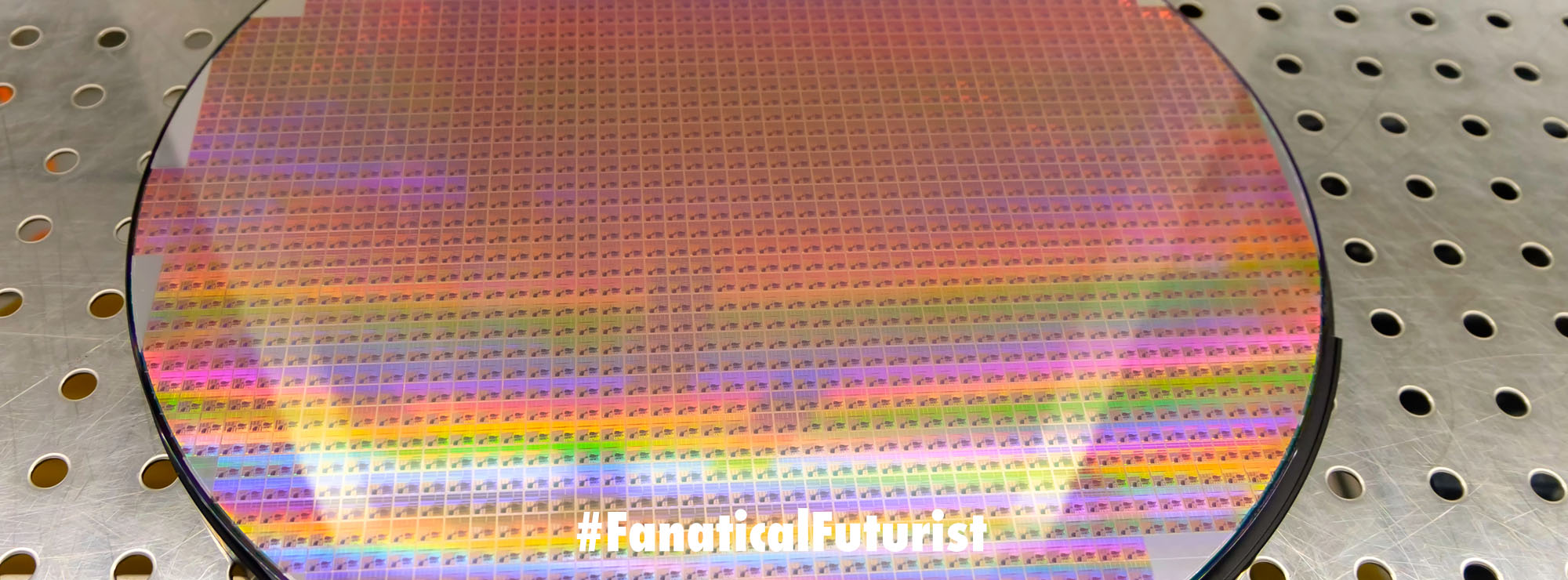
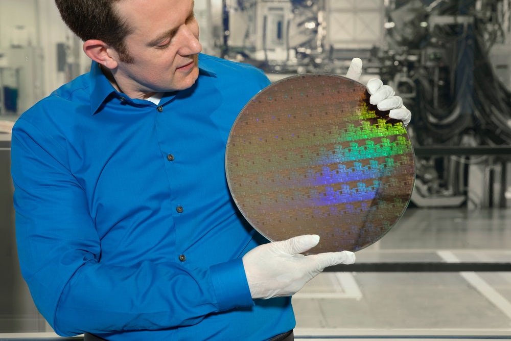
IBM, in partnership with Samsung and Global Foundries, who manufacture the chips for Qualcomm and AMD, among others, has unveiled a new process EUV lithography (Extreme Ultraviolet) process for fabricating 5nm chips that will let companies fit over 30 billion transistors onto a single computer chip.
It was only two years ago that IBM announced unveiled it’s process to fabricate 7nm chips which Samsung will likely ship beginning next year, but today’s announcement sounds like an even more important breakthrough in chip design given the fact that many people in the industry believe that Moore’s Law, the law which has governed chip design for decades, and which could be soon be replaced by Quantum Computing’s Rose’s Law, is at worst dead and at best slowing down, and that’s despite the fact that new 1nm processes are starting to appear, albeit in the labs.
The 5nm chip uses a “Gate-all-around” transistor (GAAFET), where the gate material is wrapped around a trio of horizontal silicon nanosheets, rather than today’s more usual FinFET design which uses vertical fins and which is the mainstay of all of today’s state of the art chips.
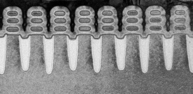
IBM has also claimed that it sees a way to scale FinFET designs down to 5nm but there’s a performance ceiling on that design because of the limits of current flow through the minuscule fins at that scale. In a way, the Gate-all-around architecture is more simple than FinFET and it’s argued it could be scaled scaled as far down as 3nm.
IBM claims that chips based on this new design will have a 40 percent performance improvement over today’s 10nm chips that are currently produced by the likes of AMD, ARM and Intel, without the need to draw any additional power. Alternatively, putting it another way, the new chips, if companies kept their performance levels at the same levels, could reduce power consumption by 75 percent.
IBM’s new process also allows for nanosheet width to be adjusted continuously in a single chip design, which means circuits can be fine tuned for power and performance in one manufacturing pass.
So Moore’s Law might be struggling, but don’t bury it yet. But, when it, or rather, silicon, does eventually run out of steam we’ll have plenty of alternative computing platforms to choose from, including Chemical, DNA, Optical, or Photonic, and, of course, Quantum computing platforms.