WHY THIS MATTERS IN BRIEF
Trying to find backdoors in components is hard, but this technology will also let companies reverse engineer all kinds of products easier.
 Love the Exponential Future? Join our XPotential Community, future proof yourself with courses from XPotential University, read about exponential tech and trends, connect, watch a keynote, or browse my blog.
When you’re making a pie it’s hard to know when the inside is in the state you want it to be. The same is true, but with much higher stakes, for microelectronic chips: How can engineers confirm that what’s inside has truly met the intent of the designers? How can a semiconductor design company tell whether its intellectual property was stolen? Much more worrisome, how can anyone be sure a kill switch or some other hardware trojan hasn’t been secretly inserted?
Today, that probing is done by grinding away each of the chip’s many layers and inspecting them using an electron microscope. It’s slow going and, of course, destructive, making this approach hardly satisfactory for anybody.
Levi works with semiconductors and Aeppli works with X-rays. So, after pondering this problem, they considered using X-rays to non-destructively image chips. You’d need to go beyond the resolution used in medical X-ray scanners. But it was clear to the duo that the needed resolution was possible. At that moment, the “Chip Scan” project was born.
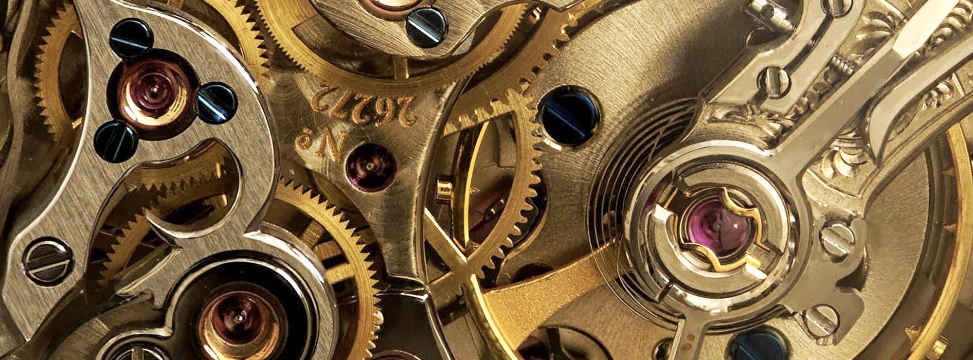
The new technology in action
Several years later and the guys have made it possible to map the entire interconnect structure of even the most advanced and complex processors without destroying them. Right now, that process takes more than a day, but improvements over the next few years should enable the mapping of entire chips within hours.
This technique, called Ptychographic X-ray Laminography, requires access to some of the world’s most powerful X-ray light sources. But most of these facilities are, conveniently, located close to where much of the advanced chip design happens. So as access to this technique expands, no flaw, failure, or fiendish trick will be able to hide.
After deciding to pursue this approach their first order of business was to establish what state-of-the-art X-ray techniques could do. That was done at the Paul Scherrer Institute (PSI) in Switzerland where Aeppli works. PSI is home to the Swiss Light Source (SLS) synchrotron, one of the 15 brightest sources of coherent X-rays built so far.
Coherent X-rays differ from what’s used in a medical or dental office in the same way that the highly collimated beam of light from a laser pointer differs from light emitted in all directions from an incandescent bulb. The SLS and similar facilities generate highly coherent beams of X-ray photons by first accelerating electrons almost to the speed of light. Then, magnetic fields deflect those electrons, inducing the production of the desired X-rays.
To see what they could do with the SLS, their multidisciplinary team bought an Intel Pentium G3260 processor from a local store for about US $50 and removed the packaging to expose the silicon – this CPU was manufactured using 22-nanometer CMOS FinFET technology.
Like all such chips, the G3260’s transistors are made of silicon, but it’s the arrangement of metal interconnects that link them up to form circuits. In a modern processor, interconnects are built in more than 15 layers, which from above look like a map of a city’s street grid. The lower layers, closer to the silicon, have incredibly fine features, spaced just nanometers apart in today’s most advanced chips. As you ascend the interconnect layers, the features become sparser and bigger, until you reach the top, where electrical contact pads connect the chip to its package.
They began our examination by cutting out a 10-micrometer-wide cylinder from the G3260. They had to take this destructive step because it greatly simplified things. Ten micrometers is less than half the penetration depth of the SLS’s photons, so with something this small they’d be able to detect enough photons passing through the pillar to determine what was inside.
They then placed the sample on a mechanical stage to rotate it about its cylindrical axis and then fired a coherent beam of X-rays through the side. As the sample rotated, they illuminated it with a pattern of overlapping 2-µm-wide spots.
At each illuminated spot, the coherent X-rays diffracted as they passed through the chip’s tortuous tower of copper interconnects, projecting a pattern onto a detector, which was stored for subsequent processing. The recorded projections contained enough information about the material through which the X-rays travelled to determine the structure in three dimensions. This approach is called ptychographic X-ray computed tomography (PXCT). Ptychography is the computational process of producing an image of something from the interference pattern of light through it.
The underlying principle behind PXCT is relatively simple, resembling the diffraction of light through slits. You might recall from your introductory physics class that if you shine a coherent beam of light through a slit onto a distant plane, the experiment produces what’s called a Fraunhofer diffraction pattern. This is a pattern of light and dark bands, or fringes, spaced proportionally to the ratio of the light’s wavelength divided by the width of the slit.
If, instead of shining light through a slit, you shine it on a pair of closely spaced objects, ones so small that they are effectively points, you will get a different pattern. It doesn’t matter where in the beam the objects are. As long as they stay the same distance from each other, you can move them around and you’d get the same pattern.
By themselves, neither of these phenomena will let you reconstruct the tangle of interconnects in a microchip. But if you combine them, you’ll start to see how it could work. Put the pair of objects within the slit. The resulting interference pattern is derived from the diffraction due to a combination of slit and object, revealing information about the width of the slit, the distance between the objects, and the relative position of the objects and the slit. If you move the two points slightly, the interference pattern shifts. And it’s that shift that allows you to calculate exactly where the objects are within the slit.
Any real sample can be treated as a set of point-like objects, which give rise to complex X-ray scattering patterns. Such patterns can be used to infer how those pointlike objects are arranged in two dimensions. And the principle can be used to map things out in three dimensions by rotating the sample within the beam, a process called tomographic reconstruction.
You need to make sure you’re set up to collect enough data to map the structure at the required resolution. Resolution is determined by the X-ray wavelength, the size of the detector, and a few other parameters. For their initial measurements with the SLS, which used 0.21-nm-wavelength X-rays, the detector had to be placed about 7 meters from the sample to reach our target resolution of 13 nm.
In March 2017, the duo demonstrated the use of PXCT for non-destructive imaging of integrated circuits by publishing some very pretty 3D images of copper interconnects in the Intel Pentium G3260 processor. Those images reveal the three-dimensional character and complexity of electrical interconnects in this CMOS integrated circuit. But they also captured interesting details such as the imperfections in the metal connections between the layers and the roughness between the copper and the silica dielectric around it.
From this proof-of-principle demonstration alone, it was clear that the technique had potential in failure analysis, design validation, and quality control. So we used PXCT to probe similarly sized cylinders cut from chips built with other companies’ technologies. The details in the resulting 3D reconstructions were like fingerprints that were unique to the ICs and also revealed much about the manufacturing processes used to fabricate the chips.
They were encouraged by our early success. But knew they could do better, by building a new type of X-ray microscope and coming up with more effective ways to improve image reconstruction using chip design and manufacturing information. They called the new technique PyXL, shorthand for ptychographic X-ray laminography.
The first thing to deal with was how to scan a whole 10-millimeter-wide chip when we had an X-ray penetration depth of only around 30 µm. They solved this problem by first tilting the chip at an angle relative to the beam. Next, they rotated the sample about the axis perpendicular to the plane of the chip. At the same time they also moved it sideways, raster fashion. This allowed them to scan all parts of the chip with the beam.
At each moment in this process, the X-rays passing through the chip are scattered by the materials inside the IC, creating a diffraction pattern. As with PXCT, diffraction patterns from overlapping illumination spots contain redundant information about what the X-rays have passed through. Imaging algorithms then infer a structure that is the most consistent with all measured diffraction patterns. From these they can reconstruct the interior of the whole chip in 3D.
Needless to say, there is plenty to worry about when developing a new kind of microscope. It must have a stable mechanical design, including precise motion stages and position measurement. And it must record in detail how the beam illuminates each spot on the chip and the ensuing diffraction patterns. Finding practical solutions to these and other issues required the efforts of a team of 14 engineers and physicists. The geometry of PyXL also required developing new algorithms to interpret the data collected. It was hard work, but by late 2018 the duo had successfully probed 16-nm ICs, publishing the results in October 2019.
In these experiments they were able to use PyXL to peel away each layer of interconnects virtually to reveal the circuits they form. As an early test, they inserted a small flaw into the design file for the interconnect layer closest to the silicon. When they compared this version of the layer with the PyXL reconstruction of the chip, the flaw was immediately obvious.
In principle, a few days of work is all they’d need to use PyXL to obtain meaningful information about the integrity of an IC manufactured in even the most advanced facilities. Today’s cutting-edge processors can have interconnects just tens of nanometers apart, and their technique can, at least in principle, produce images of structures smaller than 2 nm.
But increased resolution does take longer. Although the hardware we’ve built has the capacity to completely scan an area up to 1.2 by 1.2 centimeters at the highest resolution, doing so would be impractical. Zooming in on an area of interest would be a better use of time. In their initial experiments, a low-resolution (500-nm) scan over a square portion of a chip that was 0.3 mm on a side took 30 hours to acquire. A high-resolution (19-nm) scan of a much smaller portion of the chip, just 40 μm wide, took 60 hours.
The imaging rate is fundamentally limited by the X-ray flux available at SLS. But other facilities boast higher X-ray fluxes, and methods are in the works to boost X-ray source “brilliance” – a combination of the number of photons produced, the beam’s area, and how quickly it spreads. For example, the MAX IV Laboratory in Lund, Sweden, pioneered a way to boost its brilliance by two orders of magnitude. A further one or two orders of magnitude can be obtained by means of new X-ray optics. Combining these improvements should one day increase total flux by a factor of 10,000.
With this higher flux, they should be able to achieve a resolution of 2 nm in less time than it now takes to obtain 19-nm resolution. Our system could also survey a one-square-centimeter integrated circuit – about the size of an Apple M1 processor – at 250-nm resolution in fewer than 30 hours.
And there are other ways of boosting imaging speed and resolution, such as better stabilizing the probe beam and improving the algorithms to account for the design rules of ICs and the deformation that can result from too much X-ray exposure.
Although we can already tell a lot about an IC from just the layout of its interconnects, with further improvements we should be able to discover everything about it, including the materials it’s made of. For the 16-nm-technology node, that includes copper, aluminum, tungsten, and compounds called silicides. They might even be able to make local measurements of strain in the silicon lattice, which arises from the multilayer manufacturing processes needed to make cutting-edge devices.
Identifying materials could become particularly important, now that copper-interconnect technology is approaching its limits. In contemporary CMOS circuits, copper interconnects are susceptible to electromigration, where current can kick copper atoms out of alignment and cause voids in the structure. To counter this, the interconnects are sheathed in a barrier material. But these sheaths can be so thick that they leave little room for the copper, making the interconnects too resistive. So alternative materials, such as cobalt and ruthenium, are being explored. Because the interconnects in question are so fine, they’ll need to reach sub-10-nm resolution to distinguish them.
There’s reason to think they’ll get there. Applying PXCT and PyXL to the “connectome” of both hardware and wetware (brains) is one of the key arguments researchers around the world have made to support the construction of new and upgraded X-ray sources. In the meantime, work continues in laboratories in California and Switzerland to develop better hardware and software. So someday soon, if you’re suspicious of your new CPU or curious about a competitor’s, you could make a fly-through tour through its inner workings to make sure everything is really in its proper place …