WHY THIS MATTERS IN BRIEF
Russia is way behind China and almost everyone else in semiconductor development, but at least they have a plan …
 Love the Exponential Future? Join our XPotential Community, future proof yourself with courses from XPotential University, read about exponential tech and trends, connect, watch a keynote, or browse my blog.
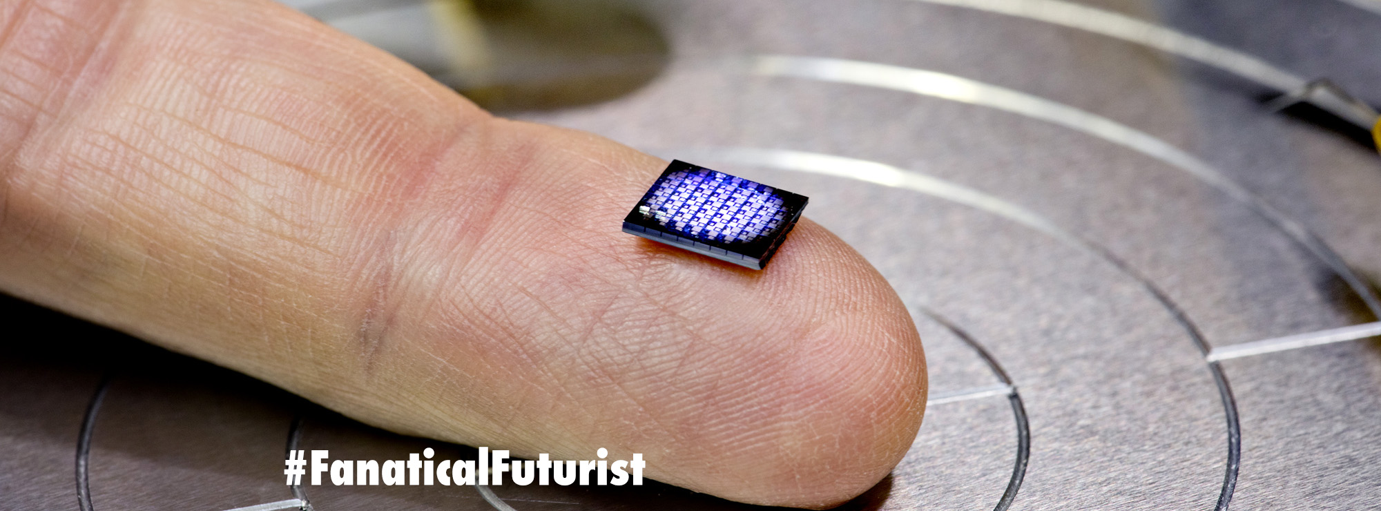
As the battle to develop new faster chips and semiconductors rages, with the US putting sanctions on China who are increasingly building out their own ecosystem, the Institute of Microstructure Physics of the Russian Academy of Sciences has laid out a long-term roadmap for domestic Extreme Ultraviolet (EUV) Lithography tools operating at a wavelength of 11.2 nm, extending the information the organization shared last December. The new project spans from 2026, utilizing 40nm manufacturing technology, and extends to 2037, incorporating sub-10nm fabrication processes. The latest roadmap looks more realistic than some previous ones, yet it still has to prove itself to be executable. Furthermore, if executable, it may not be used for commercial purposes.
The very first thing that strikes the eye is that the proposed EUV systems avoid replicating the architecture of ASML’s tools. Instead, the plan is to use an entirely different set of technologies: hybrid solid-state lasers, xenon plasma-based light sources, and mirrors made from ruthenium and beryllium (Ru/Be) that reflect light at a 11.2nm wavelength. The choice of xenon instead of tin droplets in ASML’s EUV tools eliminates debris that harms photomasks, which dramatically reduces maintenance. Meanwhile, when compared to ASML’s DUV tools, the lower complexity is meant to avoid high-pressure immersion fluids and multi-patterning steps for advanced nodes.
The roadmap includes three main stages. The first system, scheduled for 2026–2028, is a 40nm-capable lithography machine with a two-mirror objective, 10nm overlay accuracy, an exposure field of up to 3 x 3 mm, and throughput exceeding five wafers per hour. The second stage (2029–2032) introduces a 28 nm (with potential for 14 nm) scanner utilizing a four-mirror optical system. It offers 5 nm overlay precision, a 26 x 0.5 mm exposure field, and output exceeding 50 wafers per hour. The final system (2033–2036) targets sub-10 nm production with a six-mirror configuration, 2 nm overlay alignment, and field sizes of up to 26 x 2 mm. It is designed to deliver throughput above 100 wafers per hour.
In terms of resolution, these tools are expected to support a range from 65 nm down to 9 nm, matching requirements for many of today’s and tomorrow’s critical layers in 2025 – 2027. Each generation advances optical precision and scan efficiency, while presumably maintaining a significantly lower per-unit cost structure compared to ASML’s Twinscan NXE and EXE platforms.
Notably, the developers claim several unexpected benefits from using EUV for trailing nodes. However, they never mention complexities arising from using a laser with an 11.2nm length (different mirrors, different tools to polish the mirrors, different optics, different light source, different power supply units, resist, just to mention a few), which is a non-industry standard wavelength when it comes to EUV lithography.
In general, this roadmap may outline Russia’s plan to achieve self-reliance in chip production by circumventing traditional EUV limitations. However, it is unclear how executable this plan is, as it would leapfrog the entire industry, something that has yet to be proven.
Rather than targeting maximum throughput for hyperscale fabs, the tools are aimed at cost-effective adoption by smaller foundries. By offering a clean, efficient, and scalable lithography system that doesn’t require immersion or tin-based plasma, the Russian platform may also appeal to international customers who are currently excluded from ASML’s ecosystem. If fully realized, the project could enable advanced chip manufacturing for both domestic and export use at significantly lower capital and operational costs.